It’s easy to get a great camera smartphone nowadays, and consumers are spoilt for choice. But that has not always been the case. Smartphone cameras have steadily evolved, and their progress on this end has been complemented and preceded by advancements in CMOS sensor technology. You likely have read CMOS sensors in the spec sheet, but what does it mean? What is a CMOS sensor, and how does it work? We explore this in this article.
QUICK ANSWER
CMOS stands for Complementary Metal Oxide Semiconductors. It is a type of image sensor that converts light received into electrical signals. Color filters are used on top of the areas on the sensor to read color data. Then, demosaicing algorithms are applied to produce an image that can be piped forward for additional processing or use.
JUMP TO KEY SECTIONS
What is a CMOS sensor?

CMOS stands for Complementary Metal Oxide Semiconductors. CMOS sensors are image sensors that convert the light they receive into electrical signals that can then be interpreted to produce an image.
How does a CMOS sensor work?
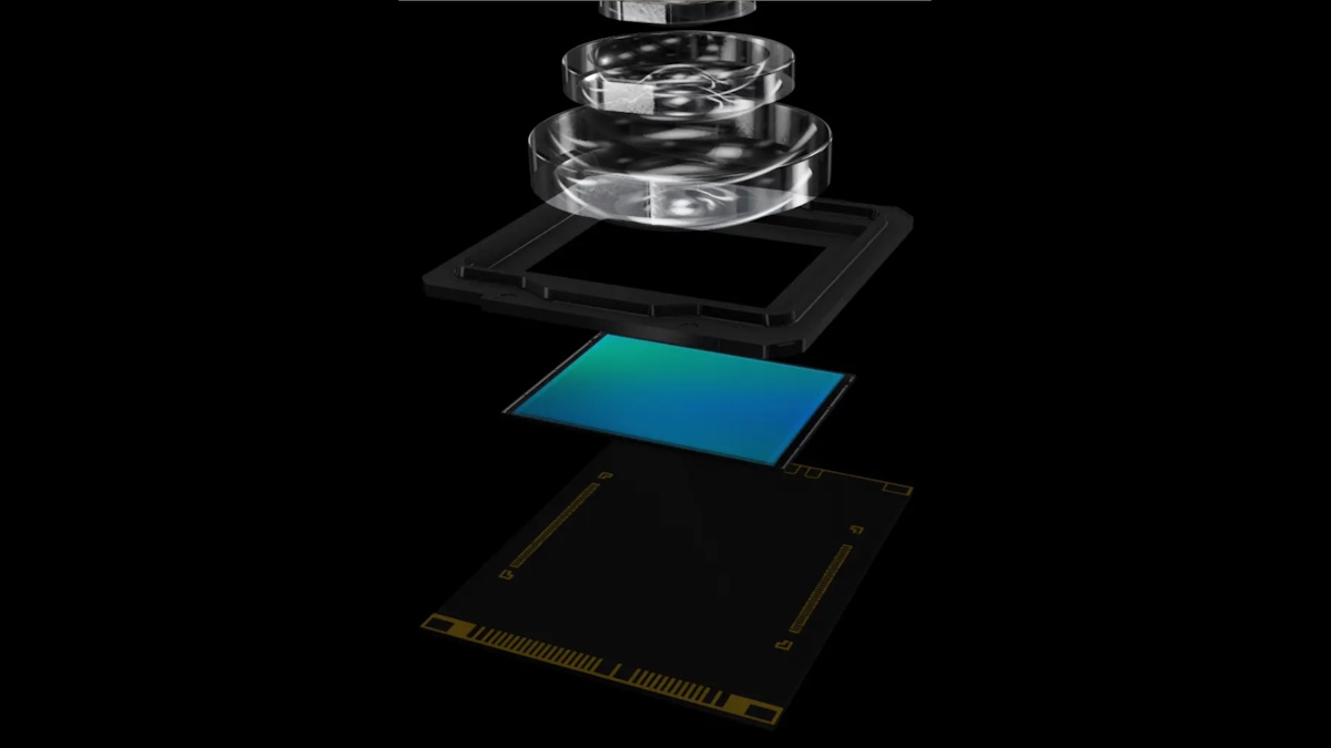
In very simplified terms, the base of a CMOS sensor is a group of “potential wells” made from a silicon wafer. Each individual potential well is a “pixel” that can receive light, react to the photons in the well, and consequently give out electrons. These electrons electronically indicate how much light has entered the well, giving the device’s brains a way to measure light.
But the mere presence of light cannot measure color. To get around this, color filters are placed over the base. These filters allow only a specific light color to enter, blocking the other colors.
This then poses another challenge. Images are made of multiple colors, and getting data for only one color will only reveal a part of the picture but not the whole.
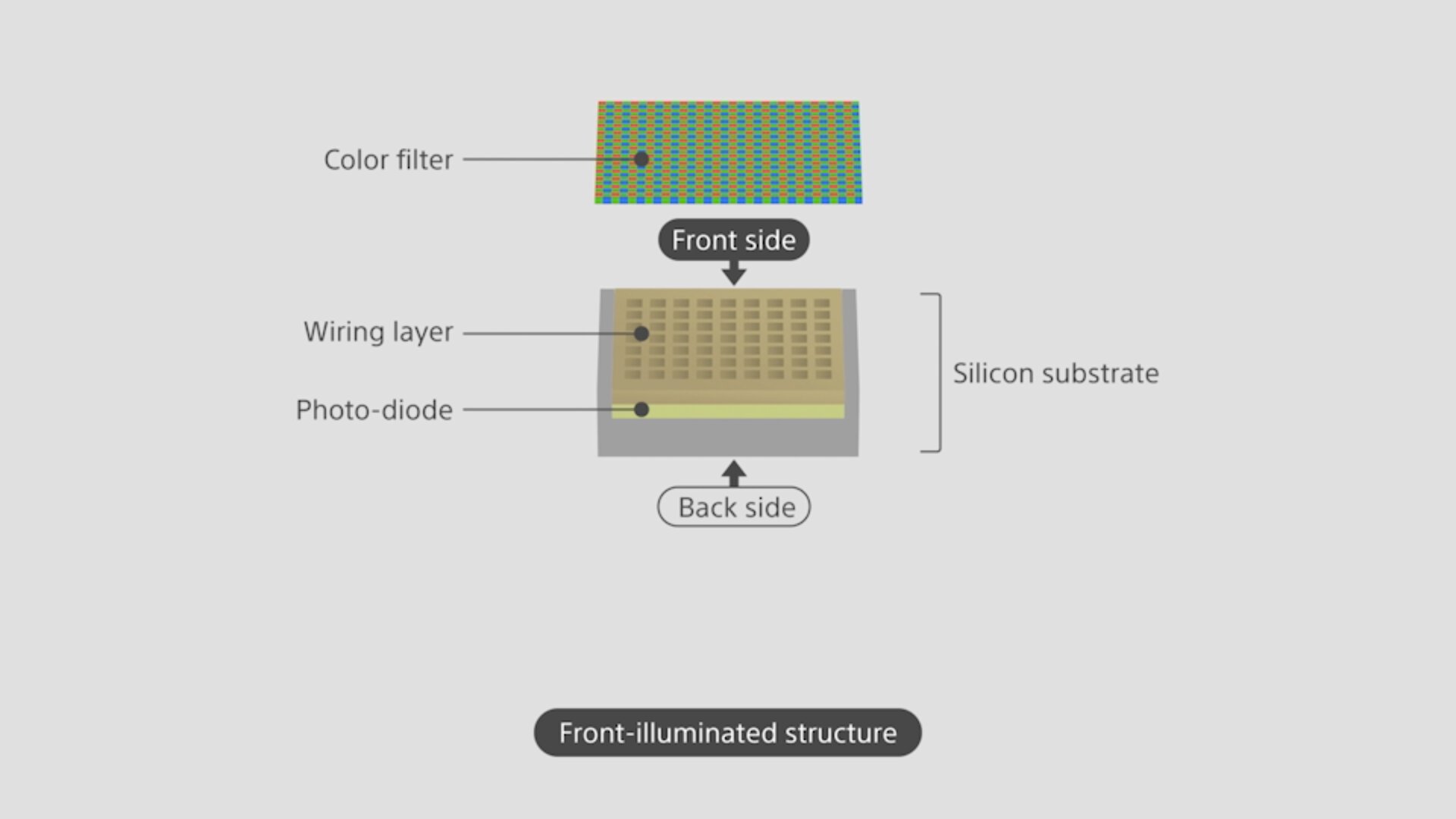
CMOS sensors work around this by alternating the color filters used in adjacent pixels and then aggregating the data from nearby wells through a process called demosaicing. So, each pixel captures only one color data; combined with its neighboring pixels, you have a good approximation of the image’s color.
How does a CMOS sensor technically work?
A CMOS sensor is basically a silicon chip that has a lot of photosensitive pockets, aka pixels. When light enters a pixel, the silicon material absorbs energy from the photons. When the material absorbs enough energy, the electrons present within try to escape their bonds, thereby producing an electric charge. This effect is called the photoelectric effect. The CMOS sensor, by this stage, has converted light to voltage.
A singular pixel can only measure how much light has entered within itself. You will thus need a plane full of adjacent pixels to determine the various areas of high and low light that have entered the pixels cumulatively.
So when a camera sensor mentions itself to be 1MP, it means there are 1 million pixels (aka 1 megapixel) on the sensor, spread 1,000 pixels by 1,000 pixels (though this distribution can vary).
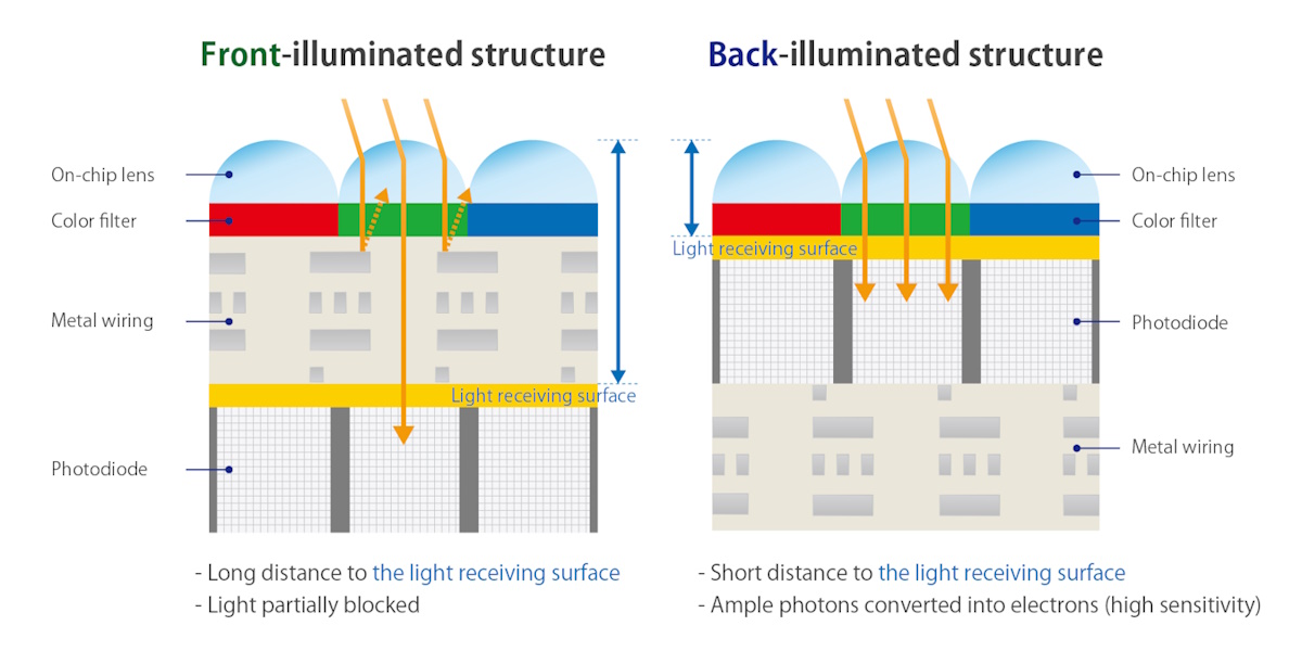
In a CMOS sensor, voltage measurement is done on a pixel level. Thus, each pixel can individually have the charge it holds read out. This differs from legacy image sensors, where the voltage was read out sequentially, row by row. The measured voltage is then passed through an ADC (analog-to-digital converter), which converts the voltage into a digital representation.
As mentioned in the simplified explanation, this voltage measured is the mere presence of light. The voltage does not contain any information regarding the color of the light that has entered it, so it cannot adequately represent an image. Image sensors work around this by using color filters on top of the pixel, allowing only a single color to reach inside the pixel.
Adjacent pixels use alternating color filters, usually in the RGBG array (Red-Green-Blue-Green), known as the Bayer filter mosaic. This sequence is used as the human eye is susceptible to green light, and the quantity of green in this arrangement is twice as much as red or blue.
Thus, each pixel records whether one of red, green, or blue light has entered into it. We end up with three layers of colors through this color filter array. Information on the other two missing colors is taken from the adjacent pixels through an interpolation process called demosaicing.
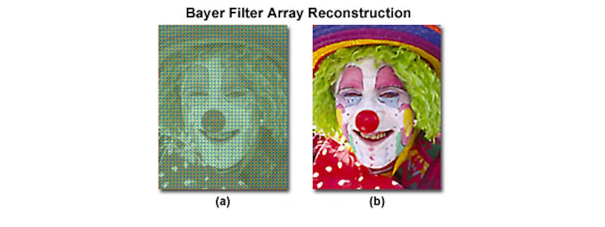
This gives us our base image, upon which smartphone OEMs can apply algorithms and other manipulations before presenting to the end user.
CMOS vs CCD sensors
CCD stands for Charge Coupled Device, a legacy sensor technology that CMOS sensors have largely phased out.
The primary difference between CCD and CMOS sensors is while CMOS sensors can measure voltage data at a per-pixel level, the CCD sensor measures this for an array of pixels (a row of pixels together). This fundamental difference between the two is what creates different use cases.
CCD sensors can create low-noise images but also require much more power. They are also expensive to produce and slower to operate as the charge needs to be read out row by row.
On the other hand, CMOS sensors are susceptible to more noise. Still, they can be manufactured on standard silicon production lines relatively cheaply, require lower power to operate, and can have their data read very quickly (since data can be read on a per-pixel level). The noise disadvantage has also been shaved off with rapid advancements in the tech, and as a result, CMOS has taken over most use cases.
FAQs
Full-frame is sensor size, which is not a direct comparison with CMOS, which is sensor technology. CMOS sensors can be full-frame or crop sensors and full-frame sensors can be CMOS or other tech.
APS-C refers to Advanced Photo System type-C, and it refers to a popular sensor size. CMOS is the sensor technology that is being used. Nikon has a special trademark for APS-C size sensors, called DX format, but it is often used interchangeably.
BSI-CMOS refers to Backside Illuminated CMOS, a subset of CMOS technology with faster readout speeds. Due to architectural differences, it can output images with lower noise.
Stacked CMOS sensors are an extension of BSI-CMOS that allows for even faster readout speeds.


